Lattice Materials provides custom-grown and machined silicon and germanium material, precision parts, and stunning optics.
In the heart of Big Sky country is a passionate crew of engineers, scientists, and manufacturing experts who serve leading defense, optics, semiconductor, and research and development companies.
We’re pleased to introduce you to Lattice Materials, one of the only United States-based providers of custom-grown silicon and germanium crystals, thin film materials, semiconductor parts, precision optics, and mirrors.
Based in Bozeman, Montana, Lattice began serving customers in 1989, providing silicon and germanium optical materials, machining, lapping and polishing, testing, and metrology.
Over the years, the company expanded its expertise and capabilities to include semiconductor support, thin film materials, mirrors, and curve generation while maintaining a strict commitment to service, precision, quality, pricing, and on-time delivery.

The Art and Science of Crystal Growth
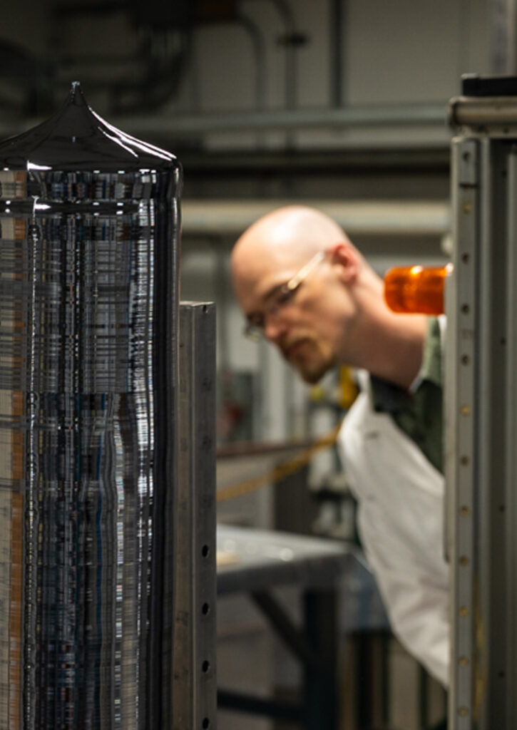
Lattice scientists have been custom-growing silicon and germanium Czochralski crystals since the company’s earliest days.
The staff scientists and technicians are well-versed in growing these crystals to demanding specifications, including hard-to-find sizes, unique orientations, custom electrical resistivity, and special optical transmissions.
Most importantly, Lattice’s parts, optics, mirrors, and components offer full traceability because every crystal is grown in the USA.

Stunning Optics
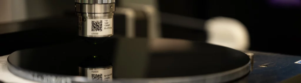
Lattice’s technicians are experts in polishing finished optical windows, lenses, and blanks for many of the world’s largest and most respected defense, automotive, and optics companies.
The company’s manufacturing crews produce round or rectangular shapes up to 17.5” (450 mm) that are polished to optical specifications better than 20/10 scratch/dig, 1/10th wave flatness, and down to 10 Å RMS. The Lattice crew can add AR, DLC, and other custom film coatings.
Further, their specialty in curved lens delivery helps clients as they build out components used in mission-critical applications.
The Lattice expertise includes round or truncated shapes up to 14” in diameter that are polished to better than 40/20 scratch/dig, 1/4 fringe flatness, and 3 Å RMS.
Supporting Technology with Excellence
Many of today’s leading technology companies call on Lattice Materials for their variety of silicon parts, custom wafer sizes, and technical expertise.
Lattice produces custom wafers of any diameter up to 14.5” and any thickness down to ½ mm with precision polishes and etching capabilities to better than 20/10 scratch/dig, 1/10 wave flatness, and down to 10 Å RMS.

A Partner to Count On
In addition to the company’s technical and manufacturing prowess, Lattice Materials boasts some of the brightest minds in the industry who are available to consult customers through the design, material selection, production, finish, and delivery process.
Plus, the Resources Library on Lattice Materials’ website provides scientific, technical, and packaging details for customers’ reference.
We invite you to visit the Lattice Materials website and reach out for any assistance.
Joining The Partner Companies
The Partner Companies welcomed Lattice Materials into its global portfolio of specialty manufacturers and solutions providers in 2016.
“Becoming part of TPC has been such a powerful experience for us all,” says Lattice Materials President Jessica Higgins. “We’ve joined some of the best precision manufacturing companies in the United States and can now offer our customers an even broader range of capabilities.”